Simviation Forums
Flight Simulator and other chat
Flight Simulator and other chat
![]() by caveman16 » Wed Dec 28, 2005 11:33 pm
by caveman16 » Wed Dec 28, 2005 11:33 pm
![]() by congo » Thu Dec 29, 2005 6:40 am
by congo » Thu Dec 29, 2005 6:40 am
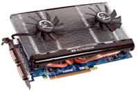 Mainboard: Asus P5K-Premium, CPU=Intel E6850 @ x8x450fsb 3.6ghz, RAM: 4gb PC8500 Team Dark, Video: NV8800GT, HDD: 2x1Tb Samsung F3 RAID-0 + 1Tb F3, PSU: Antec 550 Basiq, OS: Win7x64, Display: 24&
![]() by caveman16 » Thu Dec 29, 2005 11:01 am
by caveman16 » Thu Dec 29, 2005 11:01 am
![]() by GunnerMan » Thu Dec 29, 2005 6:27 pm
by GunnerMan » Thu Dec 29, 2005 6:27 pm

![]() by Weather_Man » Thu Dec 29, 2005 6:51 pm
by Weather_Man » Thu Dec 29, 2005 6:51 pm

![]() by congo » Fri Dec 30, 2005 4:57 am
by congo » Fri Dec 30, 2005 4:57 am
Mainboard: Asus P5K-Premium, CPU=Intel E6850 @ x8x450fsb 3.6ghz, RAM: 4gb PC8500 Team Dark, Video: NV8800GT, HDD: 2x1Tb Samsung F3 RAID-0 + 1Tb F3, PSU: Antec 550 Basiq, OS: Win7x64, Display: 24&![]() by caveman16 » Fri Jan 20, 2006 9:29 am
by caveman16 » Fri Jan 20, 2006 9:29 am
 I've copied and studied this info soooooo careful. You "GUYS" need to write a book to explain "things" so the rest of us can understand it . I "got it" much clearer than the many books I've read about building a PC. I know I'm somewhat backward - - BUT - - it is nice to understand things from the "BASIC's". Thanks again. caveman
 Users browsing this forum: No registered users and 614 guests